At the crossroads of miniaturization and sustainability in electronics assembly, Direct Metallization is redefining the performance benchmark for PCB via metallization. As global supply chains increasingly enforce Environmental, Social and Governance (ESG) requirements, traditional electroless copper processes face tremendous transformation pressure due to their complex chemistry and heavy environmental footprint.
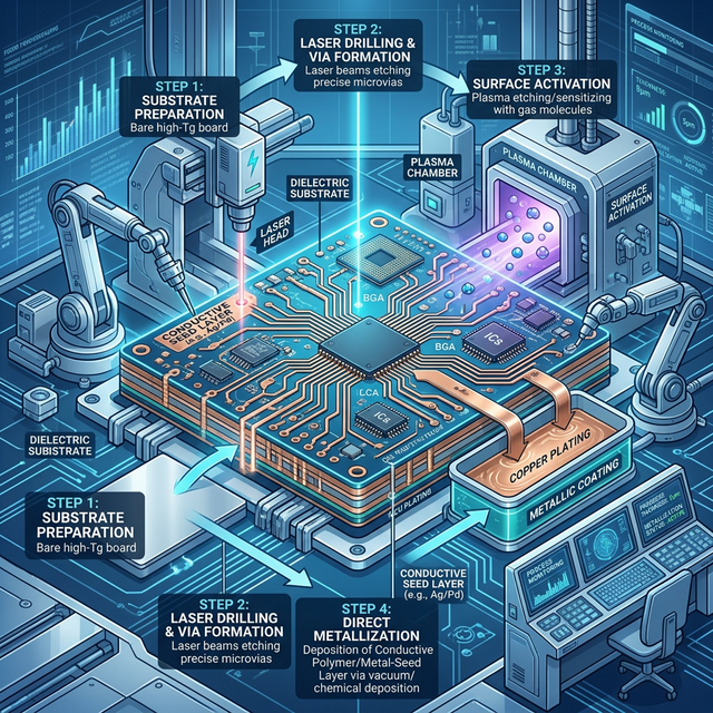
Evolution of the Core Technology Logic
Direct Metallization completely overturns the traditional "catalysis-electroless copper" pathway, instead anchoring a conductive medium layer directly on insulating via walls to enable subsequent electroplating. This innovation not only eliminates the use of formaldehyde and strong complexing agents like EDTA, but also achieves up to a 35% reduction in energy consumption by shortening the process chain.
Forward-Looking 3D Advantages
- 1. Ultimate green moat: Full compliance with RoHS and green factory evaluation systems.
- 2. Consistency of High Aspect Ratio Via Spreading: Providing more uniform copper layer connections for 5G base stations and high-layer server mainboards.
- 3. Significantly enhanced substrate compatibility: Demonstrating excellent adhesion in FPC flexible boards and multi-layer rigid-flex boards.
Alpha Support Chain: From Materials to Process
As a strategic partner of Alpha in Greater China, Junjun Tech not only provides high-end conductive medium materials but is also dedicated to providing full-stack soldering process optimization recommendations. For via wall quality after direct metallization, we recommend using Alpha flagship series solder paste and low-tension alloys to ensure solder joint integrity under extreme thermal shock.
Conclusion & Vision
Direct Metallization is no longer just a "substitute option" — it is the inevitable path towards digitalized closed-loop manufacturing. Junjun Tech will continue to partner with industry leaders to build a high-reliability, low-emission electronics manufacturing future.