Low-Silver Lead-Free Wave & Selective Low Dross

ALPHA® SACX Plus® 0307

Low-silver, lead-free alloy for wave, selective and rework applications. Engineered for improved copper dissolution performance during long hot exposure times.

Product Overview

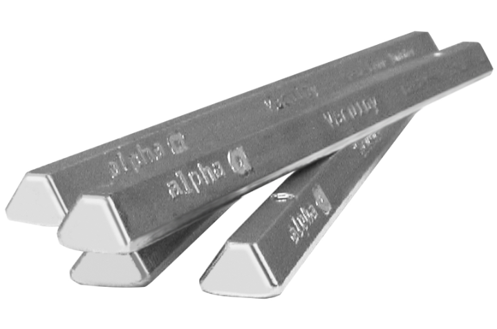
ALPHA SACX Plus 0307 is a low-silver, lead-free alloy designed as a replacement for SnPb, SAC305, and other low-silver Tin-Silver-Copper (SAC) alloys, including the original SACX 0307, in wave soldering, lead tinning, and rework processes.

Engineered for enhanced copper dissolution performance, ALPHA SACX Plus 0307 excels in applications requiring long hot exposure times, such as rework and lead tinning.

ALPHA® SACX Plus 0307

Product Features

ALPHA® SACX Plus 0307 Product Features
  • Low-Silver for Lower Material Cost
  • Low Dross Rate
  • Low Copper Dissolution
  • Excellent Mechanical Reliability
  • Fast Wetting and Wide Process Window

Wave, Selective and Lead-Free Applications

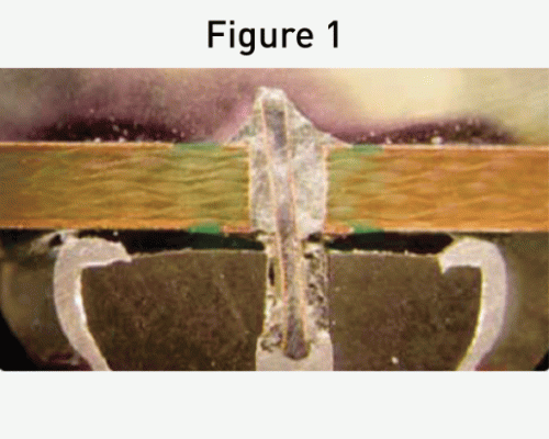
ALPHA SACX Plus 0307 is suitable for wave soldering and selective soldering for electronic assemblers interested in implementing a lead-free process. It is suitable for nearly all types of boards (single & double-sided) and works particularly well on assemblies with Organic Solderability Preservative (OSP) pad finishes that have been exposed to prior reflow excursions and where lower silver or silver free alloys have not worked.

Application Guidelines
View Detailed Product Parameters

Technical Specifications

Complies with all requirements of RoHS Directive (Article 4.1 of the European Directive 2011/65/EU). Alloy specification for Maximum Lead (Pb) Content = 0.07% SACX Plus 0307 is also available is an Ultra-Low Lead (ULL) version which contains a maximum of 0.05% Pb. All alloy properties remain the same for SACX Plus 0307 ULL.

Material Property Units Vaculoy SACX Plus 0307
Solidus Celsius 217
Liquidus Celsius 228
Hardness HV 14.1
Density g/cc 7.33
Specific Heat Capacity J/kg C 0.17
Stress at MAX Load (N/mm²) Mean 29.5
Std Dev 0.64
Elongation at failure (%) Mean 21.8
Std Dev 8.8
Thermal Expansion Coefficient (30 - 100C)/C x 10-5 1.79
(100 - 150C)/C x 10-5 2.30
Silver Content % 0.3 +0.15/-0.05
Copper Content % 0.70 +/- 0.1
Lead Content % Max 0.07%

RECOMMENDED WAVE SOLDER PROCESSING SETTING

Wave Configuration Process Parameter Suggested Process Settings
Single Wave
Pot Temperature255 to 265 °C (491 to 509 °F)
Conveyor Speed1.0 to 1.5 m/min (3.3 to 5 ft/min)
Contact Time2.3 to 2.8 seconds
Wave Height1/2 to 2/3 of board thickness
Dross RemovalOnce per 8 hour run time
Copper CheckEvery 8,000 boards until 40,000
Dual Wave
Pot Temperature255 to 265 °C (491 to 509 °F)
Conveyor Speed1.0 to 1.5 m/min (3.3 to 5 ft/min)
Contact Time3.0 to 3.5 seconds
Wave Height1/2 to 2/3 of board thickness
Dross RemovalOnce per 8 hour run time
Copper CheckEvery 8,000 boards until 40,000

These are general guidelines which have proven to yield excellent results. However, depending upon your equipment, components and circuit boards, your optimal settings may be different. To optimize your process, it is recommended to perform a design experiment, optimizing the most important variables (i.e., amount of flux applied, conveyor speed, topside preheat temperature, solder pot temperature, board orientation, etc.).

MANAGEMENT OF COPPER LEVELS IN THE SOLDER BATH

Copper should be controlled in the solder bath between 0.7% and 1.0%.

Management of the copper level in the wave solder bath is critical to ensure low defects in the soldering process. There is a tendency for the copper levels within a high tin bearing alloy wave solder bath to increase due to copper dissolution from the PCB. This effect increases based on the level of exposed copper on the assembly, as in the case of boards using OSP pad finishes.

Studies have shown a typical leaching rate of 0.01% Cu per 1000 boards. As each process is unique, this rate should be viewed as a guideline only. It is recommended that the copper is controlled at between 0.7% and max 1.0% for SACX Plus 0307 alloy. If the copper levels are higher than 1.0% then this will increase the liquidus temperature which in turn may mean that the solder bath temperature must be increased to maintain the process yields.

The copper levels in the bath can be controlled by means of adding SACX Plus 0300 to the wave solder pot. It may be the case that equilibrium can be attained by continuing with SACX Plus 0300 additions as the only means of solder top up, however each process is unique, and we would recommend regular analysis of the solder bath so that good control of copper can be maintained. This analysis service is available from Alpha, contact your local sales office for details.

RECOMMENDED ACTION LEVELS FOR WAVE SOLDER IMPURITIES

Please find below a list of recommended action levels for wave solder bath impurities. For specific action plans to bring your solder bath back to an acceptable condition please contact Alpha.

Element ACTION Levels % Notes
SnBALNo Action level.
Pb0.10RoHS Directive 2011/65/EU states a maximum Lead content of 0.1%
As0.03Levels greater than 0.03% can cause de-wetting.
Cu1.0SACX Plus 0307 is tolerant to copper levels up to 1.0%; SACX Plus 0300 copper free should be added to maintain copper levels. Levels above 1.0% may cause more bridging.
Bi0.20Lead Free alloys are tolerant to Bi up to 1.0%, however if levels above 0.20% are detected this indicates some contamination issues that should be investigated.
Zn0.003Levels greater than 0.003% may cause increased bridging and icicling, as well as, increased drossing rates in the solder bath.
Fe0.02Greater than 0.02% Iron can be an indicator of pot erosion and may cause gritty joints and the formation of FeSn2 IMC needles that can cause bridging.
Ag1.0Silver levels of 4% are used in some SAC alloys, however if the levels in SACX 0307 rise above 1% then some investigations should be held to establish the cause.
Sb0.20Lead Free alloys are tolerant to Sb up to 1.0%, however if levels above 0.20% are detected this indicates some contamination issues that should be investigated.
Ni0.05Levels greater than 0.05% may start to slow wetting and may reduce hole fill. Evaluate soldering performance if levels exceed 0.05%. Locate and eliminate source of high Ni levels.
Cd0.003RoHS Directive 2011/65/EU states a maximum Cadmium content of 0.01%. Levels of 0.003% may cause higher level of bridging and icicling.
Al0.002Levels greater than 0.002% may cause higher levels of bridging and icicling and a greater level of surface oxidation in the solder bath.